MIT engineers grow “high-rise” 3D chips
An electronic stacking technique could exponentially increase the number of transistors on chips, enabling more efficient AI hardware.

The electronics industry is approaching a limit to the number of transistors that can be packed onto the surface of a computer chip. So, chip manufacturers are looking to build up rather than out.
Instead of squeezing ever-smaller transistors onto a single surface, the industry is aiming to stack multiple surfaces of transistors and semiconducting elements — akin to turning a ranch house into a high-rise. Such multilayered chips could handle exponentially more data and carry out many more complex functions than today’s electronics.
A significant hurdle, however, is the platform on which chips are built. Today, bulky silicon wafers serve as the main scaffold on which high-quality, single-crystalline semiconducting elements are grown. Any stackable chip would have to include thick silicon “flooring” as part of each layer, slowing down any communication between functional semiconducting layers.
Now, MIT engineers have found a way around this hurdle, with a multilayered chip design that doesn’t require any silicon wafer substrates and works at temperatures low enough to preserve the underlying layer’s circuitry.
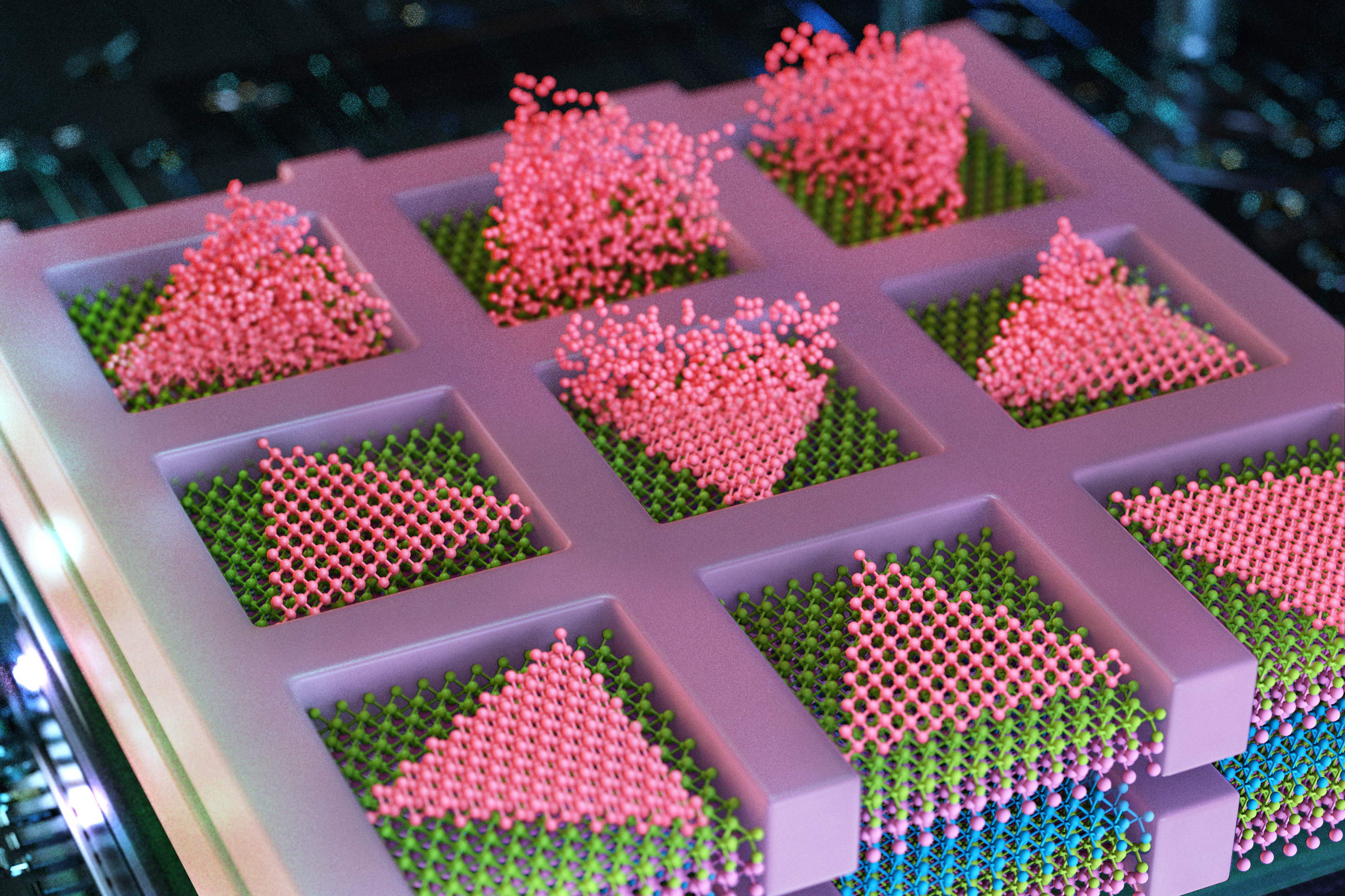
In a study appearing today in the journal Nature, the team reports using the new method to fabricate a multilayered chip with alternating layers of high-quality semiconducting material grown directly on top of each other.
The method enables engineers to build high-performance transistors and memory and logic elements on any random crystalline surface — not just on the bulky crystal scaffold of silicon wafers. Without these thick silicon substrates, multiple semiconducting layers can be in more direct contact, leading to better and faster communication and computation between layers, the researchers say.
The researchers envision that the method could be used to build AI hardware, in the form of stacked chips for laptops or wearable devices, that would be as fast and powerful as today’s supercomputers and could store huge amounts of data on par with physical data centers.
“This breakthrough opens up enormous potential for the semiconductor industry, allowing chips to be stacked without traditional limitations,” says study author Jeehwan Kim, associate professor of mechanical engineering at MIT. “This could lead to orders-of-magnitude improvements in computing power for applications in AI, logic, and memory.”
The study’s MIT co-authors include first author Ki Seok Kim, Seunghwan Seo, Doyoon Lee, Jung-El Ryu, Jekyung Kim, Jun Min Suh, June-chul Shin, Min-Kyu Song, Jin Feng, and Sangho Lee, along with collaborators from Samsung Advanced Institute of Technology, Sungkyunkwan University in South Korea, and the University of Texas at Dallas.
Seed pockets
In 2023, Kim’s group reported that they developed a method to grow high-quality semiconducting materials on amorphous surfaces, similar to the diverse topography of semiconducting circuitry on finished chips. The material that they grew was a type of 2D material known as transition-metal dichalcogenides, or TMDs, considered a promising successor to silicon for fabricating smaller, high-performance transistors. Such 2D materials can maintain their semiconducting properties even at scales as small as a single atom, whereas silicon’s performance sharply degrades.
In their previous work, the team grew TMDs on silicon wafers with amorphous coatings, as well as over existing TMDs. To encourage atoms to arrange themselves into high-quality single-crystalline form, rather than in random, polycrystalline disorder, Kim and his colleagues first covered a silicon wafer in a very thin film, or “mask” of silicon dioxide, which they patterned with tiny openings, or pockets. They then flowed a gas of atoms over the mask and found that atoms settled into the pockets as “seeds.” The pockets confined the seeds to grow in regular, single-crystalline patterns.
But at the time, the method only worked at around 900 degrees Celsius.
“You have to grow this single-crystalline material below 400 Celsius, otherwise the underlying circuitry is completely cooked and ruined,” Kim says. “So, our homework was, we had to do a similar technique at temperatures lower than 400 Celsius. If we could do that, the impact would be substantial.”
Building up
In their new work, Kim and his colleagues looked to fine-tune their method in order to grow single-crystalline 2D materials at temperatures low enough to preserve any underlying circuitry. They found a surprisingly simple solution in metallurgy — the science and craft of metal production. When metallurgists pour molten metal into a mold, the liquid slowly “nucleates,” or forms grains that grow and merge into a regularly patterned crystal that hardens into solid form. Metallurgists have found that this nucleation occurs most readily at the edges of a mold into which liquid metal is poured.
“It’s known that nucleating at the edges requires less energy — and heat,” Kim says. “So we borrowed this concept from metallurgy to utilize for future AI hardware.”
The team looked to grow single-crystalline TMDs on a silicon wafer that already has been fabricated with transistor circuitry. They first covered the circuitry with a mask of silicon dioxide, just as in their previous work. They then deposited “seeds” of TMD at the edges of each of the mask’s pockets and found that these edge seeds grew into single-crystalline material at temperatures as low as 380 degrees Celsius, compared to seeds that started growing in the center, away from the edges of each pocket, which required higher temperatures to form single-crystalline material.
Going a step further, the researchers used the new method to fabricate a multilayered chip with alternating layers of two different TMDs — molybdenum disulfide, a promising material candidate for fabricating n-type transistors; and tungsten diselenide, a material that has potential for being made into p-type transistors. Both p- and n-type transistors are the electronic building blocks for carrying out any logic operation. The team was able to grow both materials in single-crystalline form, directly on top of each other, without requiring any intermediate silicon wafers. Kim says the method will effectively double the density of a chip’s semiconducting elements, and particularly, metal-oxide semiconductor (CMOS), which is a basic building block of a modern logic circuitry.
“A product realized by our technique is not only a 3D logic chip but also 3D memory and their combinations,” Kim says. “With our growth-based monolithic 3D method, you could grow tens to hundreds of logic and memory layers, right on top of each other, and they would be able to communicate very well.”
“Conventional 3D chips have been fabricated with silicon wafers in-between, by drilling holes through the wafer — a process which limits the number of stacked layers, vertical alignment resolution, and yields,” first author Kiseok Kim adds. “Our growth-based method addresses all of those issues at once.”
To commercialize their stackable chip design further, Kim has recently spun off a company, FS2 (Future Semiconductor 2D materials).
“We so far show a concept at a small-scale device arrays,” he says. “The next step is scaling up to show professional AI chip operation.”
This research is supported, in part, by Samsung Advanced Institute of Technology and the U.S. Air Force Office of Scientific Research.


